Memory system
Load store unite
The LSU implementation is characterised by :
LQ / SQ : Usually, 16 of each
Load from AGU : To reduce the load latency, if the LQ has nothing for the load pipeline, then the AGU can directly provide its fresh calculation without passing by the LQ registers
Load Hit speculation : In order to reduce the load to use latency (to 3 cycles instead of 6), there is a cache hit predictor, speculatively waking up depending instructions
Hazard prediction : For store, both address and data are provided through the issue queue. So, a late data will also create a late address, potential creating store to load hazard. To reduce that occurence, a hazard predictor was added to the loads.
Store to load bypass : If a given load depend on a single store of the same size, then the load pipeline may bypass the store value instead of waiting for the store writeback
Parallel memory translation : For loads, to reduce the latency, the memory translation run in parallel of the cache read.
Shared address pipeline : Load and store use the same pipeline to translate the virtual address and check for hazards.
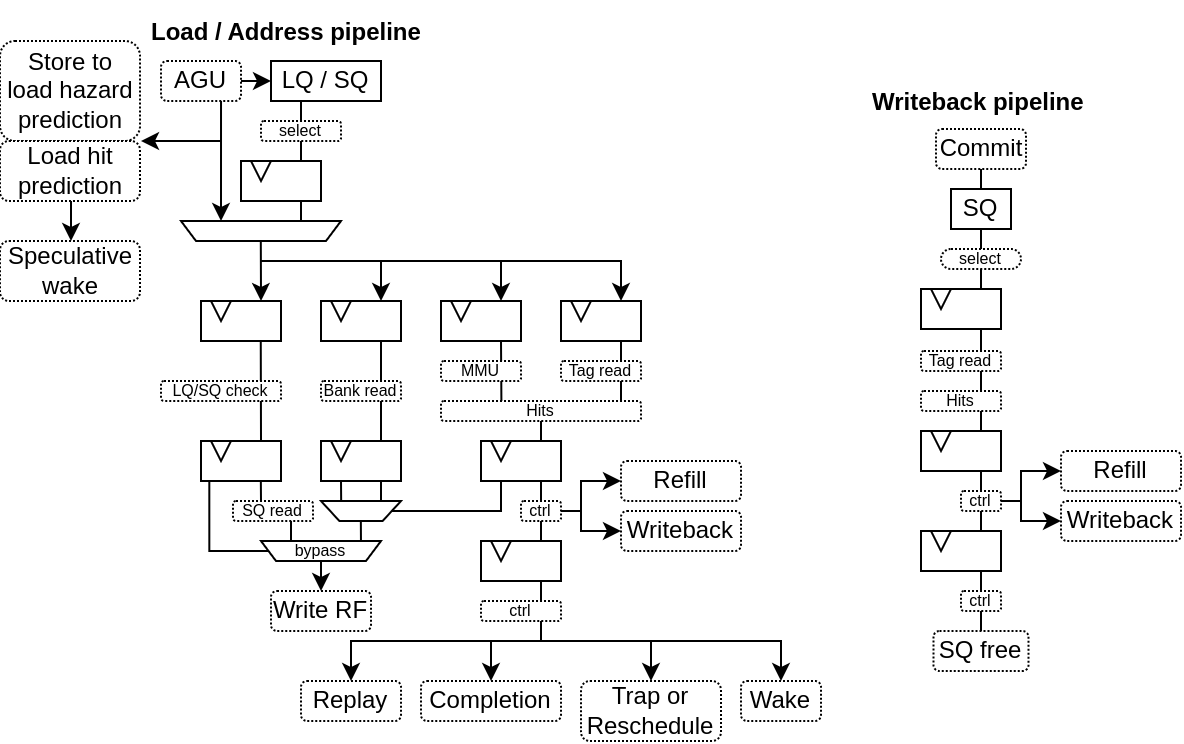
Here is a few illustrations of the shared and the writeback pipeline :
MMU
The MMU implementation is characterised by :
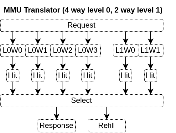
2D organisation : For each level of the page table a parameterizable number of direct mapped ways of translation cache can be specified.
Hardware refilled : Because that’s cheap
Caches direct hit : Allows the instruction cache to check its way tags directly against the MMU TLB storage in order to improve timings (at the cost of area)
For RV32, the default configuration is to have :
4 ways * 32 entries of level 0 (4KB pages) TLB
2 ways * 32 entries of level 1 (4MB pages) TLB
The area of the TLB cache is kept low by inferring each way into a distributed ram.
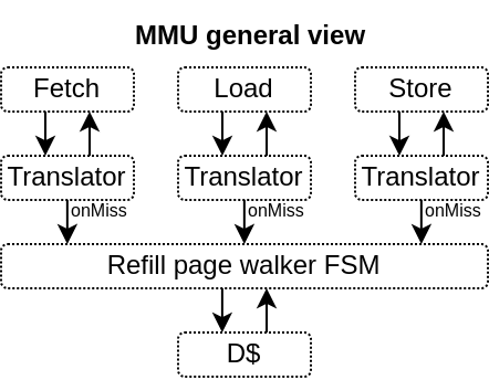
Here is a few illustrations of the MMU design
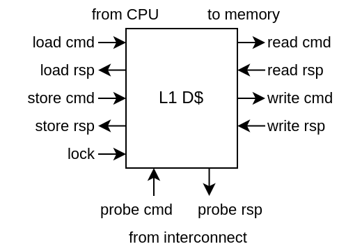
Coherency
The memory coherency is implemented the following way on the CPU :
Blocks of memory (in the data cache) have permission levels (unloaded < shared < unique[dirty])
Shared permission only allows read-only access
Unique permission allows read/write accesses
When the data cache want to upgrade its permission, he will issue an acquire request (on the read bus)
When the data cache want to free-up space, he will send a release request (on the write bus)
The interconnect can downgrade the data cache permission on a given address (on the probe bus)
Probe requests are handled by reusing the data cache store pipeline
To allow the CPU to do atomic load/store access, a locking interface allows to prevent a given address permission downgrade
While NaxRiscv native data cache interface to the memory is custom, it is made to be bridged into Tilelink.
From a SoC perspective, you can pick either a L2 coherent cache or a cacheless coherency hub to connect multiple masters.
L2 cache
The L2 cache has the following characteristics :
Provide Tilelink interfaces (up for CPUS/DMA, down for the memories)
Inclusive with L1 (only D$ for NaxRiscv), so it only send necessary probes, but always has a copy of the L1.
PLRU line eviction
non-blocking
multi-way
Data memory implemented as simple dual port ram (FPGA friendly)
Support selective cachability of access in function of address / source (usefull to not cache video DMA accesses)
In its default configuration, its timings are : - Hit latency 5 cycles - Miss latency penality 4 cycles
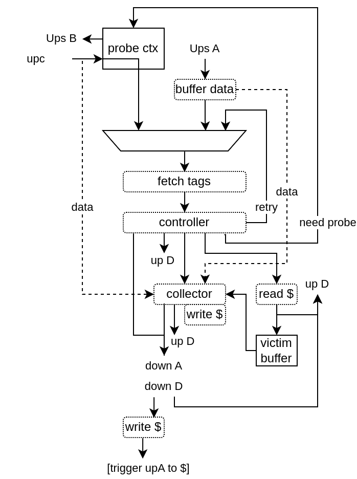
Its architecture is mostly :
Requests goes into a centralized tags fetcher / controller
That controller can feed a few pipelines / FSM, as described bellow :
Probe controller when it is needed to remove data from a l1 cache, may be required to evict a L2 cache line or to aquire unique permissions
Read down.a when we need to either refill a cache line or do a uncached read access
Send direct responses to up.d, for instance on a up.c.release
Send request to the data collector, which can then write the main memory / cache and also send data to up.d
Send request to the read cache, used on cache hit and cache evict